Monday, August 4, 2025

why in lower metal layers the resistance /capacitance increases.


In lower metal layers the cross sectional area of the metal decreases. As the cross sectional area decreases the resistance increases.  So the resistance is more in lower metal layers. 

Hence to reduce the delay its suggested to move to higher metal layers. 


Also lower metal layers are more prone to coupling cap as the distance between the two metal layers is less. If you want to avoid more cap move to higher layers or increase the distance between the two metals routed side by side. 


From the formula below if the distance between two metals decreases the capacitance increases. 

A is area of contact of two metals. 

D is the distance. 

E0 is the permitivity of free space in general here it is permitivity of the dielectric / the permitiivity of the material between the two metal layers. 


Sunday, January 26, 2025

why cant we define two logically exclusive clocks as physically exclusive

 What are logically exclusive clocks

             They are clocks which are not active at the same time. They might be two clocks which are muxed a the mux with a select pin. 


set_clock_groups -logically_exclusive CLK1 CLK2


Take the example below there are two clocks CLK1 and CLK2. 

Here the two clocks at the mux output would be exclusive to each other. 

But you see at the input A first the CLK1 is propagating to few sinks 

There might be crosstalk physically between the CLK1 clock arm going to the input registers and that of the mux output clocks CLK1/ CLK2. 


Here if we defined two clocks as logically asynchronous then the crosstalk would be calculated between the CLK1 and CLK2


Here if we could have defined the two clocks as physically exclusive there would be no crosstalk calculated. 


physically exclusive 

               These are clocks which do not exist at the same time on the chip. They might be a scan shift clock and a func clock.  These two clcoks do not exist at the same time on the chip.   

Thursday, March 28, 2024

How to identify the point which is to be skewed for tile to tile interface from timing reports

 Need for skewing. Skewing need to be done in the following cases 

  • High skew would increase the number of buffers getting added in the lowsvs corners 
  • Lowsvs setup is critical and each buffer added in lowsvs would add 200ps and same would only give 18ps or less in high vt corners. 
  • Memory paths which need to be balanced would be critical and they mostly need to be skewed 


How to identify the point which need to be skewed. 

  • Most likely these would be mux outputs. 
  • We can identify this by a crude way by filtering without a design knowledge by using the following simple command 
Steps 
  • The below command would give you the common pins which are repeated n number of times. 
  • Pick up the points from below and check if the skewing can be done at the below points. 
  • Identify if these are outside the block A and block B where they can be skewed at the top interface 
  • This would reduce the analysis time. 
  • If you have design knowledge you can directly identify the points which can be skewed based on design knowledge


Wednesday, March 27, 2024

debugging high latency during CTS

 During CTS we often see multiple clocks getting balanced. Sometimes we also find clocks which are not be balanced getting balanced by the CTS engine. 

CTS engine tries to balance the clocks based upon all the clocks reaching the end point or sink pin

Step1 : Get all the clocks reaching the path with high latency sink pin using the following sink pin. 

Step2: identify muxes in the clock path 

Step3:  check clocks on b pin 

Step4: check clocks on a pin 

step5: check the case value on the mux sel pin

If there is no definition of the case_value on the sel pin. Then ideally there should have been two generated clocks defined on the output of the z pin and defined logically asynchronous to resolve the issue.


 Check all clocks on the sink pin 

pt_shell> get_attribute [get_pins  {module/u_cmux2_SIZE_ONLY/z} ] clocks

{"CLKM1_long_latency_clk", "CLKM1_main_clk"}


report the clock path using the below clock and identify mux in the path by reporting the problematic clock 

report_clock_timing  -to  {mux/reg[1]/clk} -type latency -clock  main_clock -verbose

Check the clocks on b pin of mux 

pt_shell> get_attribute [get_pins  {module/u_cmux2_SIZE_ONLY/b} ] clocks

{"CLKM1_main_clk"}

Check clocks on a pin of the mux 

pt_shell> get_attribute [get_pins  {module/u_cmux2_SIZE_ONLY/a} ] clocks

{"CLKM1_long_latency_clk"}

Check case value on the mux ( If the case value is not defined then both clocks get propagated 

pt_shell> get_attribute [get_pins  {module/u_cmux2_SIZE_ONLY/sel} ] case_value

==> no case value defined


create the generated clocks at the mux output with the two clocks on A pin and B pin 

create_generated_clock -name CLKM1_main_clk_DIV1 -source [get_ports \
 {main_port}] 
  -divide_by 1  -add -master_clock [get_clocks {CLKM1_main_clk}] 
 [get_pins -hsc module/u_cmux2_SIZE_ONLY/z}] 


create_generated_clock -name long_latency_clk_DIV1 -source [get_ports \
 {main_port}] 
  -divide_by 1  -add -master_clock [get_clocks {CLKM1_long_latency_clk}] 
 [get_pins -hsc module/u_cmux2_SIZE_ONLY/z}] 


set_clock_groups -logically_exclusive -group [get_clocks CLKM1_main_clk_DIV1 ] -group [get_clocks CLKM1_long_latency_clk ] 

Issue fixed ? Share your thoughts on how else can we fix this issue and ways of debugging. Pros and cons of those ways of fixing. 

Wednesday, October 31, 2018

Advanced On Chip Variation


Environment Conditions. 
               Just like all people on globe does not experience same environment conditions -all transistors on chip does not experience the same environment conditions which influence their functioning. 
Image result for globe picture with sunny and cold weather
Voltage and Temperature 
               These include variation in voltage which is applied to the transistors and temperature at that portion of the transistor. 

Width or shape of transistors. (Process) 

              Different people across the globe are built differently. People in Germany and Russia have their average height different from people in India.

Similar way the transistor may also be on different regions on die and chip. For the same region due to process variation, the width of transistor might be different in in different areas of the chip.

        This caused the delay to vary across the different regions on the chip.

We also fix timing across the maximum and minimum operating as operating conditions for the chip to function by taking these as setup and hold corners.

Image result for transistor delay variation with voltage and temperature
On chip Variation 

              To address these issues of variation in delay of transistors we basically add delay in transistors by adding a blanket value on each transistor delay to address these variations.

Advanced On Chip Variation

         Applying a blanket value of derate would be more pessimistic for your design.
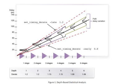
AOCV tries to address two types of variations

1. Random Variation.
                As name says random variations are those which cannot be predicted. Like the metal thickness at that region, dioxide thickness , implant doses.

  •  Random variations are proportional to the depth and they decrease proportionally based on depth. 
  •  For example the if we put in the a pessimism of 10ps derate on a cell for random variation then 8 stages will have around 80ps of 
  •  But 80ps is too pessimistic for the overall path since the overall chance of each cell in the path suffering 10ps derate is less. 
  • Hence we decide the random variation based on the depth of the cell within the path and reduce it as the depth decreases. 


2. Systematic Variation
                   Systematic variation are based on the distance. They include gate length, gate width and interconnect width etc.


  • The more the distance of the devices physically on the die, the more is the derate applied on the device. 
  • Since the devices on different regions of the die experience  PVT differently like temperature across the globe is different regions. 


Saturday, July 8, 2017

virtual clocks and their usage

Virtual Clocks
               By definition a virtual clock is a clock which does not have a port. Which is not a real clock but it mimics the functionality of a real clock.  It is advantageous to use these for optimization by giving different values of jitter and uncertainity along with
               

Use of virtual clocks gives us the following advantages while modelling the


  1. Specify the clock latencies with respect to virtual clocks with different values compared to real clocks in your design. 
  2. Gives flexibility to check IO timing separately as by default different path groups are created for different clocks.. 
  3. Perform the budgeting by adjusting the IO delays and the clock latencies on them and perform your optimization accordingly.
  4. It also gives you the flexibility to give uncertanity and jitter values differently for your optimization and timing calculation purposes


           Below is how your IO delays can be modeled based with the help of virtual clocks.
1. step 1 create the virtual clocks
2. model the input delays and output delays with respect to the virtual clocks.
3. apply the clock latencies by the virtual clocks.


create_clock -name CLK1 -period 3.236 -waveform { 0 1.618 } [get_ports {O_CLK1}]
set_clock_transition 0.150 [get_clocks {CLK1}]
set_clock_uncertainty -setup 0.110 [get_clocks {CLK1}]
set_clock_latency 2.200 [get_clocks {CLK1}]

create_clock -name VIRT_CLK1 -period 3.236 -waveform { 0 1.618 }
set_clock_transition 0.150 [get_clocks {VIRT_CLK1}]
set_clock_uncertainty -setup 0.110 [get_clocks {VIRT_CLK1}]
set_clock_latency 2.200 [get_clocks {VIRT_CLK1}]

set_input_delay 1.6 -clock [get_clocks {VIRT_CLK1}] [get_ports {O_CLK}]

Friday, October 4, 2013

DRC LVS cleaning procedure

Cleaning DRC LVS can be harrowing experience if you do not know which target to address first and which to address next.
You can follow this order for making best out of your time