Question ?
Why are we shifting to FinFET technology. Whats need ?
For years now the MOSFET size has been drastically decreasing so that we could cram in more and more transistors in a single piece of die to reduce the area and to improve the productivity.
But remember everything has its own side effects. As we go on decreasing the gate length the control of gate over the channel beneath it decreases and hence the leakage current increases. This is due to a phenomena called as sub threshold current.
First let us understand what is happening inside a MOSFET through an analogy. Im mosfet the electrons flow from source drain with gate as control. The gate creates channel for the electrons to flow. It generally creates a mirror charge for the channel flow.
This can be viewed as water flowing through a pipe which is squeezed in the middle by your hand on one side ( which is here a gate) which is obstructing the water flow. Now
As the distance between drain and source decreases by decreasing the gate length, the substrate region which offers off resistance when switch is OFF in between drain and source decreases. Hence the resistance of the switch decreases, therefore more leakage current starts to flow through the switch when the switch is OFF.

Sub threshold current.
At lower nodes where the distance between drain and source reduces the conduction from source to drain is mainly due to diffusion of electrons rather than drifting of electrons. This means that the channel can never be turned off as there would always be some conduction through diffusion of electrons.

 Point here to remember is that the Fin is sitting on top of substrate and the channel which is formed is completely isolated from the substrate. So obviously there would be no leakage current which flows through the substrate when the transistor is OFF unlike the planar transistor . Which means we have almost achieved a NO leakage transistor.
 In other words, the water flowing through the pipe is being controlled on all sides by the valve which is present on all sides. So there is no leakage flowing in the down part unlike the earlier planar transistor. Hence the problem was solved intelligently.
Why are we shifting to FinFET technology. Whats need ?
For years now the MOSFET size has been drastically decreasing so that we could cram in more and more transistors in a single piece of die to reduce the area and to improve the productivity.
But remember everything has its own side effects. As we go on decreasing the gate length the control of gate over the channel beneath it decreases and hence the leakage current increases. This is due to a phenomena called as sub threshold current.
First let us understand what is happening inside a MOSFET through an analogy. Im mosfet the electrons flow from source drain with gate as control. The gate creates channel for the electrons to flow. It generally creates a mirror charge for the channel flow.
This can be viewed as water flowing through a pipe which is squeezed in the middle by your hand on one side ( which is here a gate) which is obstructing the water flow. Now
As the distance between drain and source decreases by decreasing the gate length, the substrate region which offers off resistance when switch is OFF in between drain and source decreases. Hence the resistance of the switch decreases, therefore more leakage current starts to flow through the switch when the switch is OFF.

More the distance between source and drain, more is the resistance it can offer and hence less leakage. But remember reducing gate length is required for fitting in more transistors and reducing the chip area and die size. So we are left with no option here either we have to compromise on leakage or on area.
A gate is in general like a valve which controls the flow through the channel. As you remove the channel you are closing the valve and turning off the transistor. If you have to create a channel then you should open the valve.
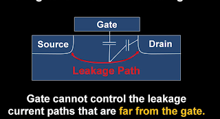
Why is leakage current present in standard planar MOSFET?
In standard planar transistor as the transistor sizes are decreasing the source and drain come closer. Hence there will always be some leakage current flowing through the substrate from source to drain without the influence of gate. It is called sub threshold leakage current. It happens under weaker gate voltages or when the gate is off.
At lower nodes where the distance between drain and source reduces the conduction from source to drain is mainly due to diffusion of electrons rather than drifting of electrons. This means that the channel can never be turned off as there would always be some conduction through diffusion of electrons.

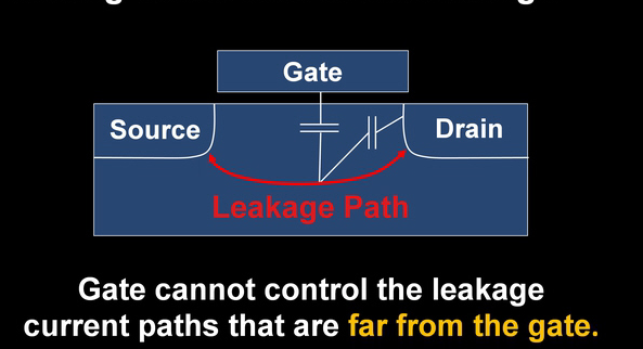
Remember that the leakage path exists far away from the gate and the gate has no control over it.
"It means valve cannot control the water flow which is far away from iself. This gives rise to leakage "
This limitation can be solved with the help of
FINFET transistor
This is when the finfet technology comes with a promising feature
In FINFET transistor the gate is on three sides of the FIN. A fin is a set of drain and source cutting through the gate. Now when the transistor is on the channel gets formed on all sides ( remember in planar mosfet channel only gets formed on one side ) and heavy rush of current flows through it.
 Point here to remember is that the Fin is sitting on top of substrate and the channel which is formed is completely isolated from the substrate. So obviously there would be no leakage current which flows through the substrate when the transistor is OFF unlike the planar transistor . Which means we have almost achieved a NO leakage transistor.
